
In-Circuit Serial Programmer
Contents
Project Overview
A Microchip programmer typically appropriates a couple of Microcontroller (MCU) data lines during its programming process. It uses one data line for a clock and the other for data. Microchip offers developers a few different options to cope with this requirement.
The socket option [1][2] entails first physically placing an MCU into a socket on a separate development board in order to program it. Afterward the MCU is then physically moved to the production board where it is either shoved into another socket or soldered into place.
A second option is to use Microchip's In-Circuit Serial Programming™ on a device already soldered to a production board. The easiest way to accomplish this is to dedicate the pertinent clock and data lines to ICSP and leave them unused by your application circuit.
When data lines are at a premium and can not be left unused, you must turn to a third alternative. In this case the data lines are isolated from the application circuit during programming. This project shows how to build an isolation circuit to achieve the third alternative.
Circuit Design
Microchip's In-Circuit Serial Programming™ (ICSP™) Guide [3] talks about how to implement ICSP. This project focuses on the chapter entitled "TB016 How to Implement ICSP™ Using PIC16F8X FLASH MCUs."
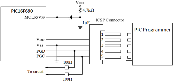
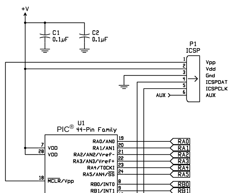
Figure 1 shows a typical application circuit from the pertinent chapter in the Guide. As an aside, it's always interesting when vendors fail to follow their own guidelines. Figure 2 shows a partial schematic of Microchip's own implementation of ISCP on its 44-Pin Demo Board. [4] Note the absence of a resistor, capacitor, and Schottky-type diode on the line between the ICSP's Vpp pin and the MCU's MCLR/Vpp pin in Figure 2.
Regardless of Microchip's mixed signals, this project follows the guidelines suggested by the ICSP Guide. In addition, Chapter 3 of Microchip's PICkit™ 2 Microcontroller Programmer User's Guide [6] and Olin Lathrop's ICSP Notes [6] both offer additional insights into ICSP. This project's schematic is shown in Figure 3.
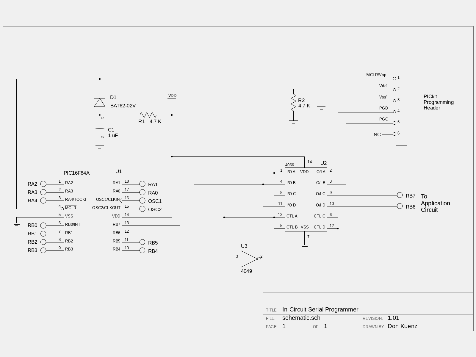
Figure 3. Schematic diagram. (Click on the schematic a couple of times to enlarge.)
In the circuit, U1 functions as a handy MCU target. Although it happens to be a venerable PIC16F84A [7], there's nothing special about it. Any other similar MCU ought work, provided you use the proper pins. Note the 4.7 kΩ resistor, 1 μF capacitor, and BAT62-02V Schottky-type diode on the line between the PIC16F84's MCLR pin and the ICSP's MCLR/Vpp pin, as recommended by the Guide. Also note the isolation between the ICSP connector's Vdd' and the application circuit's VDD.
U2 provides application circuit isolation. It's a CD4066B 4-channel analog switch [8]. U3 inverts Vdd' in order properly gate the application circuit to the MCU when the ICSP is not in use. It's a CD4049UB CMOS Hex Inverting Buffer/Converter [9].
Construction
The circuit's prototyped on the breadboard shown below in Figure 4. The remainder of the prototype board's populated with keyboard, LED, and LCD display circuits. These latter circuits are mostly cropped out of the image.
The row of three ICs with one connector in the middle, on the right side of Figure 4, comprise most of the ICSP circuit. The ICSP connector's the second package from left, in the row. The diode and resistors are located around the fuzzy black electrolytic capacitor, which appears above the fourth and last element in the row.
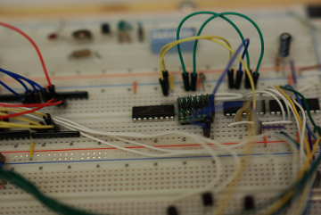
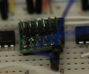
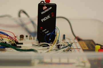
Figure 6. PICkit 2 connected to circuit.
Figure 5 shows a closeup of the ICSP connector. It's fashioned from a single SIP connector soldered to the top of universal perfboard, with two single SIPs soldered underneath, one SIP for each side of the breadboard's "valley."
The circuit's shown in action, with a PICkit 2 connected, in Figure 6. Pin 1 is the rightmost pin. Its perfboard position is marked with a Sharpie for easy identification and orientation.
Final Comments
The circuit functions as designed. It activates its isolation circuitry when programmer software drives the ICSP's Vdd' (pin 2) high (5 VDC). It restores RB7 and RB6's connection to the application after the programmer software drives pin 2 low.
Here's the procedure to program a MCU:
- Attach PICkit 2 to ICSP connector.
- Apply 5VDC to pin 2 to engage isolation.
- Program the MCU.
Use this procedure to restore a MCU to operation:
- Apply ground to pin 2 to remove isolation.
- Cycle (assert then release) MCLR to restore MCU to operation.
- Detach PICkit 2 from ICSP connector.
Notes
- [1] Microchip sockets at Mouser
- [2] Microchip sockets at DigiKey
- [3] In-Circuit Serial Programming™ (ICSP™) Guide
- [4] 44-Pin Demo User's Guide
- [5] PICkit™ 2 Microcontroller Programmer User's Guide
- [6] Olin Lathrop's ICSP Notes
- [7] PIC16F84A Data Sheet
- [8] CD4066B 4-channel analog switch
- [9] CD4049UB CMOS Hex Inverting Buffer/Converter
Bill of Materials
| Component | Description | Qty |
|---|---|---|
| R1,R2 | 4.7 kΩ resistor | 2 |
| C1 | 1 μF, 100 V electrolytic capacitor | 1 |
| D1 | BAT62-02V diode | 1 |
| U1 | PIC16F84A microcontoller | 1 |
| U2 | CD4066BCN CMOS Quad Bilateral Switch | 1 |
| U4 | CD4049UBE CMOS Hex Buffer/Converters | 1 |
© 2020 Don Kuenz